INDUSTRY SOLUTION: SEMICONDUCTOR
Precision for the Nanoscale
The semiconductor industry demands the ultimate in precision, purity, and cleanliness. We provide expert CNC machining of advanced materials for components used in every stage of wafer fabrication and handling.
Manufacturing for Wafer Fab and Beyond
Our components are used in critical semiconductor equipment where performance and purity are essential.
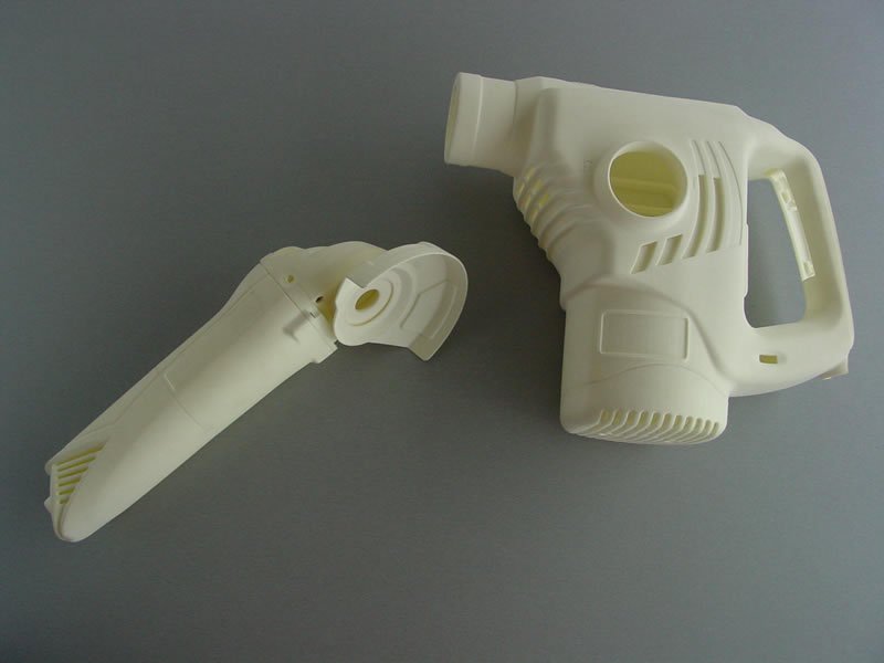
Wafer Handling Equipment
We machine components for robotic wafer handlers, end-effectors, and sorting equipment from materials that are cleanroom-compatible and non-contaminating.
Process Chamber Components
We produce parts for process chambers used in deposition, etching, and lithography, including gas delivery manifolds, showerheads, and vacuum chucks.
Test & Inspection Fixtures
We manufacture high-precision test sockets, probe card stiffeners, and fixtures from dimensionally stable, static-dissipative materials for final chip testing.
Materials for a Contamination-Free Environment
Material selection in the semiconductor industry is driven by purity, low outgassing, and resistance to aggressive process chemicals.
- High-Purity Aluminum (6061): A workhorse material for structural components, brackets, and chamber walls.
- Stainless Steel (316L): Used for its excellent corrosion resistance to process chemicals and its ability to be polished to a very smooth, cleanable surface.
- PEEK: Offers excellent chemical resistance, high purity, and low outgassing, making it ideal for wafer handling components and high-voltage insulators.
- Ceramics (e.g., Alumina): We can machine technical ceramics for components that require extreme stiffness, high thermal stability, and excellent electrical insulation.
Semiconductor Manufacturing FAQ
What kind of tolerances can you hold?
The semiconductor industry requires some of the tightest tolerances in manufacturing. With our advanced CNC machines and metrology equipment, we can hold tolerances down to ±0.010 mm or even tighter on critical features. We can also control geometric features like flatness and parallelism to exacting standards.
How do you handle part cleanliness?
We understand that cleanliness is critical. We use specialized coolants and handling procedures to prevent contamination. After machining, parts go through a multi-stage cleaning and inspection process and can be packaged in a clean environment to ensure they are ready for use in your cleanroom.
What is "outgassing"?
Outgassing is the release of trapped gases from a solid material, especially when it's in a vacuum. In semiconductor process chambers, outgassing can release unwanted contaminants that can ruin wafers. We use materials with very low outgassing properties, like PEEK and high-purity metals, to prevent this.